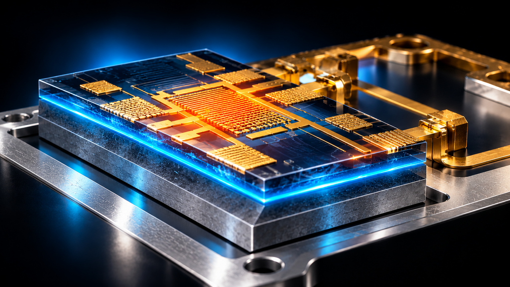
ISRONIX is developing a heterogeneous semiconductor integration platform
that combines a thin GaAs active device region with a high-thermal-conductivity
SiC substrate.
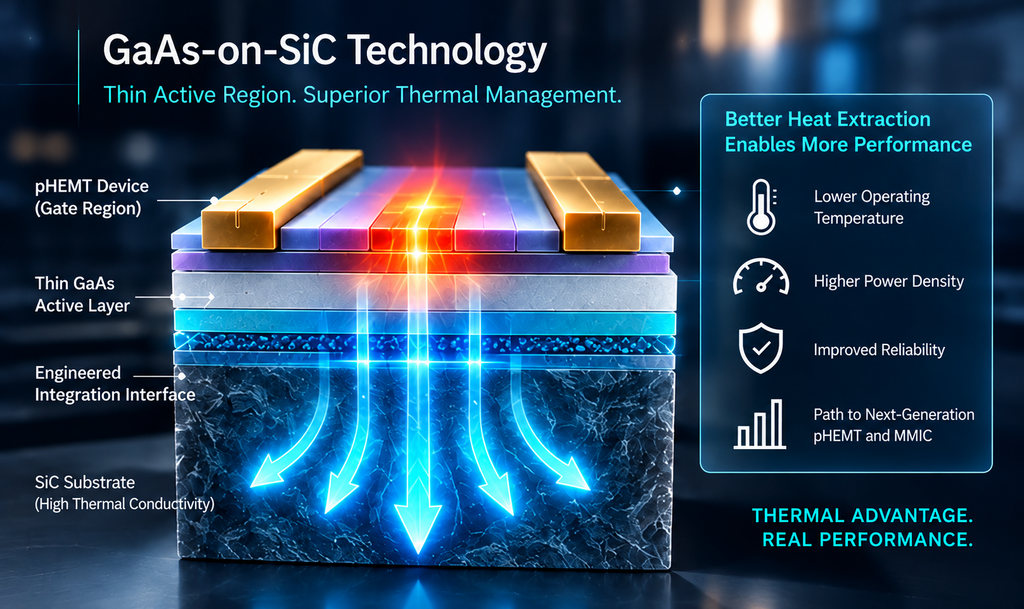
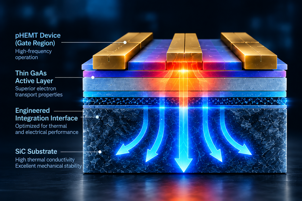
By creating a more efficient thermal path from the active region into the SiC substrate,
the platform is designed to reduce device temperature and provide greater thermal operating headroom for high-power and high-frequency applications.
This integration approach establishes a foundation for next-generation GaAs RF
power devices with improved thermal performance, higher power density potential,
and enhanced reliability.
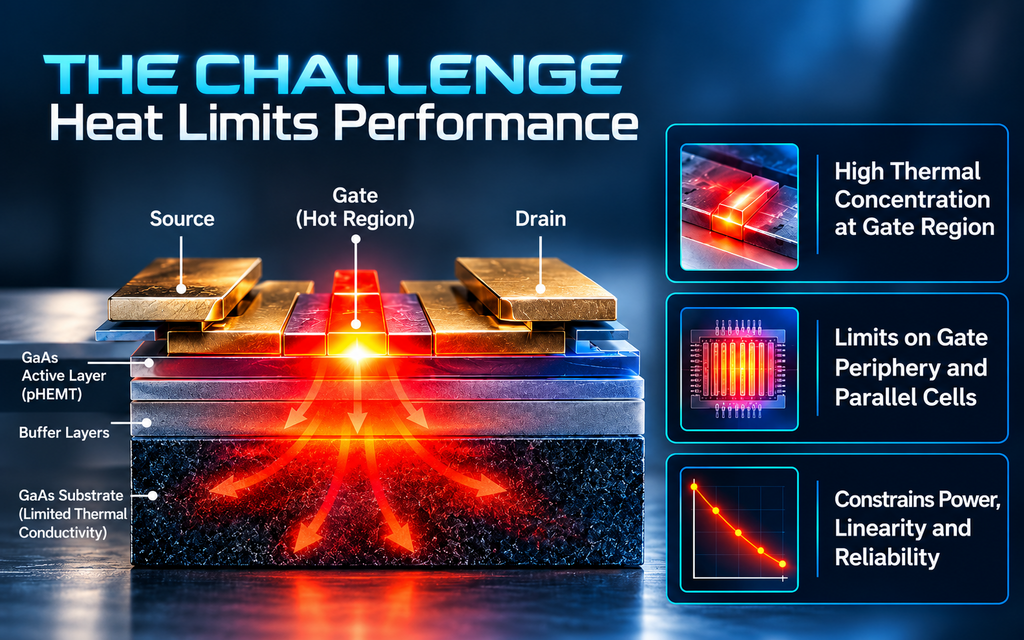
In conventional GaAs pHEMTs, heat is concentrated near the gate region
and must travel through materials with limited thermal conductivity.
As device power increases, this localized thermal resistance raises channel temperature, restricting power density, linearity and long-term reliability.
Because the heat originates within a highly localized active region, conventional cooling approaches cannot fully eliminate the thermal bottleneck.
Overcoming this limitation requires a more efficient heat extraction path directly from the active device region.
ISRONIX is engineering a shorter thermal path between the GaAs active
region and the high-thermal-conductivity SiC substrate, aiming to improve
heat extraction efficiency.
The high thermal conductivity of SiC spreads heat laterally and vertically, reducing localized thermal concentration and improving heat removal
from the active region.
ISRONIX integrates the GaAs device structure with a high-thermal-conductivity SiC substrate, creating a shorter and more efficient path for heat extraction from the active region.
Engineer and optimize the GaAs–SiC
integration interface for thermal and
structural performance.
➜
Develop and refine the bonding process to create a robust GaAs–SiC integrated structure.
➜
Establish reproducible processes to advance integrated structures toward functional RF devices.
➜
Fabricate and evaluate test structures to validate electrical, thermal and RF performance.
GaAs-on-SiC for next-generation RF power devices
ISRONIX is developing a heterogeneous GaAs-on-SiC platform that combines the RF performance of GaAs with the superior thermal conductivity of SiC through an engineered integration interface, enabling more efficient heat extraction and higher power density.